Chiplet Verification: Why Multi-Die Designs Change Everything
Chiplet verification is not just SoC verification repeated across multiple dies. Multi-die systems introduce die-to-die interfaces, package-level effects, coherency, power and thermal coupling, manufacturing test, firmware, software, and post-silicon diagnosis challenges.
Chiplet-based design is often introduced as a practical response to the limits of monolithic SoC scaling. Instead of putting every function on one large die, a system can be partitioned into compute dies, I/O dies, memory dies, accelerator dies, or base dies, and then assembled through advanced packaging and die-to-die interconnects.
Architecturally, this is powerful. It allows different process nodes, reuse of proven dies, larger effective systems, and potentially better yield economics.
From a verification perspective, however, chiplets do not simply turn one large SoC verification problem into several smaller ones. The system boundary is split across dies, but the system behavior remains integrated.
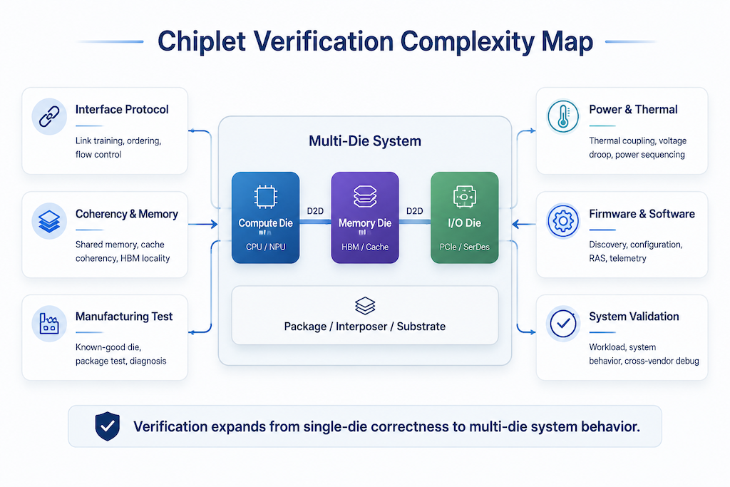
That is the essential challenge of chiplet verification: correctness is no longer confined to the RTL inside one die. It spans die-to-die protocols, package behavior, coherency, power and thermal interactions, manufacturing test, firmware, software, diagnostics, and post-silicon validation.
The following diagram summarizes the expanded verification surface.
1. Chiplets Change the Verification Boundary
In a traditional monolithic SoC, most interactions occur inside a single die. The design may still be extremely complex: CPUs, NoC fabrics, cache coherency, DMA engines, DDR controllers, PCIe, security blocks, low-power domains, firmware, drivers, and system software can all interact in difficult ways.
But the system is still largely verified within a unified design and implementation boundary.
Chiplet-based systems break that boundary.
A complete product may combine a compute die, an I/O die, a memory die, and one or more accelerators. These dies may be designed by different teams, implemented on different process nodes, or sourced from different organizations. They are then connected through a package, interposer, substrate, or another advanced integration technology.
The verification question changes from:
Does this SoC work correctly?
to:
Do these independently complex dies behave as one correct and reliable system after assembly?
That shift sounds small, but it changes many layers of the verification plan.
2. Die-to-Die Interfaces Are Not Just Another Bus
A common simplification is to treat a die-to-die interface as another high-speed bus. That is not enough.
On-chip buses and NoC links operate within one die's physical and design assumptions. A die-to-die link must cross package structures, bumps, interposer routing, clocking boundaries, power states, repair mechanisms, and sometimes different ownership boundaries.
Verification must cover more than functional packet transfer.
Important questions include:
- Does link training converge reliably?
- What happens when lanes are degraded or repaired?
- Are retry, ordering, and flow-control rules preserved under stress?
- Can error detection and recovery operate without system-level deadlock?
- Do low-power transitions preserve protocol state?
- Are reset, clock, and power sequences compatible across dies?
These are not isolated protocol questions. A failure in the die-to-die link can look like a software timeout, a coherency violation, a memory corruption, a performance collapse, or a post-silicon reliability issue.
This is why die-to-die verification requires protocol checking, traffic stress, error injection, power-state testing, package-aware assumptions, and post-silicon observability planning.
3. Coherency and Memory Behavior Become More Difficult
Many chiplet systems distribute compute, memory, cache, and I/O functions across multiple dies. That distribution increases architectural flexibility, but it also makes memory behavior harder to verify.
A multi-die system may need to support shared memory, cache coherency, HBM access, accelerator data movement, and I/O traffic across die boundaries. Even if each die behaves correctly in isolation, the assembled system can still fail under realistic traffic.
The difficult cases often appear when several effects interact:
- outstanding transactions across multiple dies;
- coherency state transitions under heavy traffic;
- memory locality and HBM bandwidth pressure;
- link-level retry and backpressure;
- software-driven cache maintenance;
- quality-of-service policies across compute and I/O dies.
This is one reason chiplet verification is not a simple extension of IP verification. Some failures emerge only when multiple agents, multiple dies, and real software-driven traffic interact.
4. Package, Power, and Thermal Effects Enter the Verification Conversation
In traditional RTL verification, package, power integrity, and thermal behavior are often treated as neighboring disciplines. They matter, but they are not always central to day-to-day functional verification.
Chiplet-based systems bring these effects closer to the verification plan.
Several dies in one package can interact thermally and electrically. A compute die running a high-power workload may heat a nearby memory die. A high-speed I/O die may create local power noise. A power-state transition in one die may affect the stability of a die-to-die link.
This does not mean RTL verification engineers must replace thermal or power-integrity experts. It means verification planning must ask how these effects can influence functional behavior.
Examples include:
- Does the system preserve protocol correctness during power-state transitions?
- Can firmware sequence power, reset, and link initialization safely?
- Does thermal throttling interact with QoS or real-time workload requirements?
- Can one die reset while the rest of the system remains recoverable?
In chiplet systems, functional correctness, power management, thermal behavior, and system firmware are more tightly connected.
5. Manufacturing Test and Diagnosis Become First-Class Concerns
Testing a monolithic SoC is already a major engineering problem. Chiplets add another layer: known-good die, package-level test, die-to-die connectivity test, repair, binning, yield learning, and system-level diagnosis.
A die can pass standalone test and still fail after assembly. The failure may be caused by package defects, interconnect issues, bump problems, marginal lanes, power delivery, thermal stress, or subtle system interactions.
As a result, verification must consider not only whether the system works, but also whether it can be tested and diagnosed when it does not work.
This changes the importance of DFT, BIST, scan, JTAG, 3D test access concepts such as IEEE 1838-style access architecture, link diagnostics, error counters, trace buffers, and post-silicon logs.
The key question is no longer only:
Can this design pass its functional tests?
It is also:
When this multi-die system fails, can we tell where and why?
Without enough observability and diagnostic structure, post-silicon debug can become extremely expensive.
6. Firmware and Software Become the System Glue
A chiplet system does not automatically become one coherent platform when power is applied. Firmware and system software must discover dies, configure links, manage power states, read telemetry, handle errors, and expose the assembled system to the operating system and runtime software.
This makes software part of the verification target.
During boot, firmware may need to answer questions such as:
- Which dies are present?
- Did each die initialize correctly?
- Are die-to-die links trained and repaired?
- Is memory available and mapped correctly?
- Are error counters clean?
- Are thermal and power policies enabled?
At runtime, software may need to handle corrected errors, uncorrected errors, link degradation, telemetry events, workload migration, or partial recovery.
These flows cannot be fully verified by local RTL tests alone. They require software-driven verification across simulation, emulation, FPGA prototyping, virtual platforms, and silicon validation.
7. Multi-Source Integration Changes Responsibility Boundaries
Chiplets are attractive partly because they enable reuse and mix-and-match integration. But that same property changes verification responsibility.
If a bug is inside a single IP block, ownership is usually clear. If a failure occurs between two dies from different teams or suppliers, the question becomes harder:
- Did both sides interpret the interface specification the same way?
- Are timing and power assumptions compatible?
- Are reset and low-power sequences aligned?
- Is the package model accurate enough?
- Is the firmware configuration valid for this die combination?
- Are compliance tests sufficient for interoperability?
The verification plan must define these boundaries early.
A robust chiplet program needs clear assumptions, compliance suites, interoperability tests, configuration matrices, error-injection plans, version tracking, and shared debug conventions.
Otherwise, integration debug becomes a negotiation problem as much as a technical problem.
8. Verification Platforms Must Work Together
It is rarely practical for a single platform to cover chiplet verification end to end.
RTL simulation remains essential for detailed protocol behavior, local logic, assertions, corner cases, and interface checkers. Formal verification is useful for protocol invariants, flow-control safety, ordering rules, and deadlock-related properties. Emulation supports large-scale multi-die RTL execution, firmware flows, driver bring-up, and system interaction debug. FPGA prototyping enables faster software execution, real I/O, and longer workloads. Silicon validation confirms the real assembled package and feeds lessons back into the verification environment.
The important question is not which platform is best. The better question is whether verification assets can move across platforms.
Examples include:
- protocol checkers;
- traffic generators;
- error-injection scenarios;
- firmware diagnostics;
- driver smoke tests;
- telemetry logs;
- performance counters;
- debug scripts.
The more reusable these assets are, the more likely the team can converge risks before and after silicon.
9. Where Complexity Actually Increases
| Dimension | Monolithic SoC Verification | Chiplet / Multi-Die Verification |
|---|---|---|
| Design boundary | Mostly one die | Multiple dies plus package and system-level assumptions |
| Interface verification | On-chip buses, NoC, external interfaces | Die-to-die links, compatibility, retry, repair, error recovery |
| Memory behavior | On-die coherency and external memory | Cross-die coherency, HBM locality, QoS, bandwidth contention |
| Power and thermal | Low-power verification and physical analysis | Cross-die thermal coupling, power sequencing, runtime management |
| Test and diagnosis | DFT, BIST, scan, silicon debug | Known-good die, package test, link diagnosis, repair, fault isolation |
| Software role | Boot, driver, configuration | Die discovery, link management, RAS, telemetry, runtime policy |
| Collaboration | Usually one SoC ownership boundary | Multiple teams, suppliers, versions, and configuration matrices |
The complexity increase is not just proportional to the number of dies. It comes from new interaction surfaces, new failure modes, and new ownership boundaries.
10. What This Means for Verification Engineers
Chiplet verification does not make traditional verification skills obsolete. It makes them more connected.
Protocol knowledge, UVM, assertions, coverage, formal methods, low-power verification, CDC, DFT awareness, software-driven testing, and post-silicon debug are still important. But engineers must also understand how their local verification scope contributes to the behavior of the assembled multi-die system.
The most effective teams will be those that can connect:
- interface verification with package assumptions;
- coherency verification with software traffic;
- power management with firmware sequencing;
- DFT with post-silicon diagnosis;
- emulation and FPGA prototyping with bring-up workflows.
No individual engineer needs to own every domain. But the verification strategy must acknowledge all of them.
Conclusion
Chiplet verification becomes significantly more complex because correctness moves beyond one die. It spans RTL, die-to-die interfaces, package behavior, coherency, power and thermal interaction, manufacturing test, firmware, software, and post-silicon diagnosis.
The challenge is not simply verifying more blocks. The challenge is proving that independently complex dies can behave as one reliable system under real operating conditions.
For multi-die designs, verification closure is no longer only about local RTL confidence. It is about system evidence across the full lifecycle of the product.